Nanomaterials
Nanomaterial Synthesis
Molecular precursors can be used for coatings and nanostructures owning different functional properties. In our laboratory, inorganic films and nanostructures are predominantly deposited by chemical vapour deposition (CVD) techniques at reduced pressure, including cold-wall CVD and focused electron beam induced deposition (FEBID). The morphology of the resulting nanoscale coatings or nanostructures is influenced by several parameters, such as precursor feedstock, substrate temperature and the inherent material properties as well as the overall pressure of the system. In addition, solvent-based approaches, such as microwave processing, are used to prepare nanoparticles and nanowires. The structural and chemical analysis of these inorganic structures include XRD, SEM, TEM, EDX, EELS etc..
In general, distinct differences in decomposition tendencies for thermal and electron-induced fragmentation processes have to be considered.
Direct-Write Method for Nanomaterial Synthesis (FEBID/FIBID)
| Focused electron beam induced deposition (FEBID) and focused ion beam induced deposition (FIBID) are elegant techniques for the deposition of nanoscale features on surfaces.
In principle, FEBID could be considered as an electron-induced CVD technique with spatial reaction control by the electron beam. Therefore, the site-selective formation of either layer-type deposits or dots on a surface or even pillars is enabled. Alternatively, complex 3D geometries can be realised by a software-assisted pattern generator. Even though FEBID has evolved and matured, there are still considerable efforts required to provide a wide platform for deposition control, automatisation as well as a broader choice of suitable precursors. Our current research focuses on the development and understanding of precursors for FEBID. The electron-molecule interactions and implications on the deposits composition can be summarized as illustrated in the following schematic. 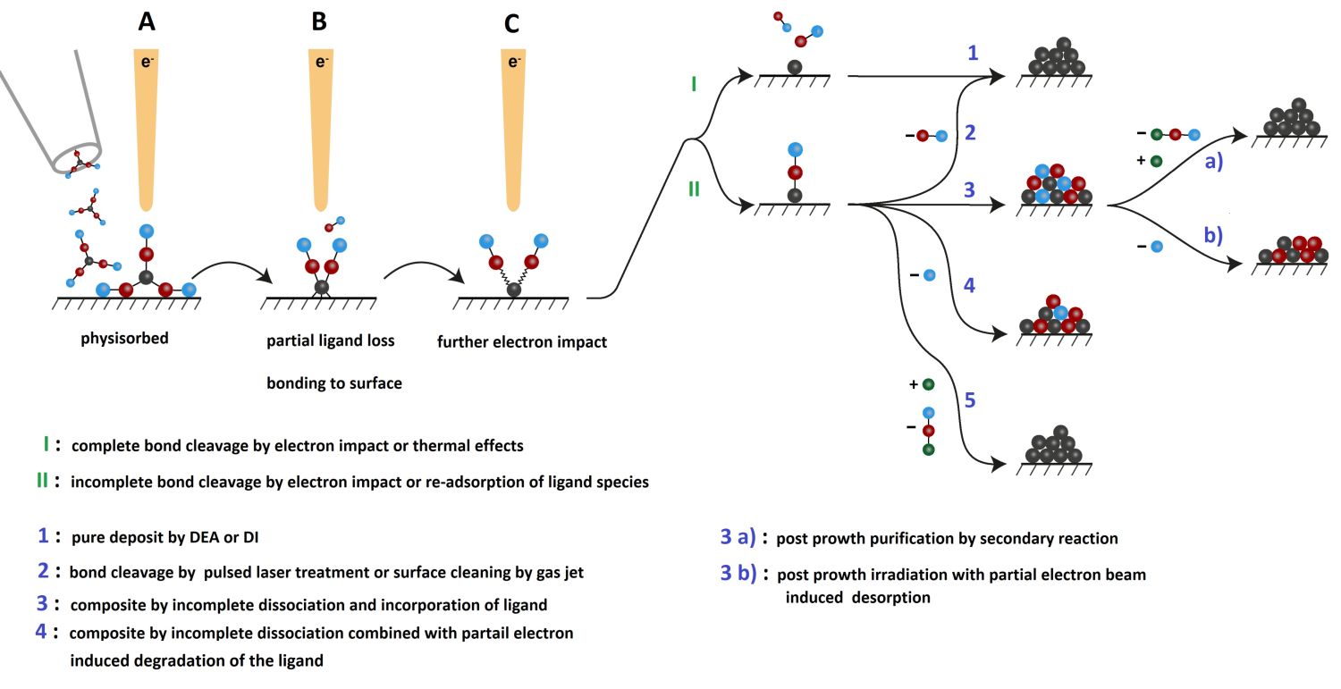
Review / Perspective: 1.) "Precursors for Direct-Write Nanofabrication with Electrons" S. Barth*, M. Huth, F. Jungwirth J. Mater. Chem. C 2020, 8, 15884-15919. 2.) Living up to its potential — Direct-write nanofabrication with focused electron beams" M. Huth,* F. Porrati, S. Barth J. Appl. Phys. 2021, 130, 170901. Selected papers: 7.) " Direct writing of cobalt silicide nanostructures using single-source precursors" F. Jungwirth, F. Porrati, A. G. Schuck, M. Huth, S. Barth* ACS Appl. Mater. Interf. 2021, 13, 48252–48259. 6.) Temperature-Dependent Growth Characteristics of Nb- and CoFe-Based Nanostructures by Direct-Write Using Focused Electron Beam-Induced Deposition M. Huth,* F. Porrati, P. Gruszka, S. Barth Micromachines 2020, 11, 8. 5.) “Crystalline niobium carbide superconducting nanowires prepared by focused ion beam direct writing” F. Porrati, S. Barth, R. Sachser, O. V. Dobrovolskiy, A. Seybert, A.S. Frangakis, M. Huth* ACS Nano2019, 13, 6287-6296. 4.)Binary Mn-Si nanostructures prepared by focused electron beam induced deposition from the precursor SiH3Mn(CO)5' F. Porrati,* S. Barth, R. Sachser, F. Jungwirth, M. Eltsov, A. Frangakis, M. Huth* J. Appl. Phys D 2018, 51, 455301. 3.) Direct-write of free-form 3D nanostructures with controlled magnetic frustration L. Keller, M. K. I. Al Mamoori, J. Pieper, C. Gspan, I. Stockem, C. Schroeder, S. Barth, R. Winkler, H. Plank, M. Pohlit, J. Mueller, M. Huth* Sci. Rep. 2018, 8, 6160. 2.)Electron Interactions with the heteronuclear carbonyl precursor (H2FeRu3(CO)13): from fundamental gas phase and surface science studies to focused electron beam induced deposition R. K. T P, P. Weirich, L. Hrachowina, M. Hanefeld, R. Bjornsson, H. R. Hrodmarsson, S. Barth, D. H. Fairbrother, M. Huth, O. Ingólfsson* Beilstein J. Nanotechnol. 2018, 9, 555-579. 1.)Direct writing of CoFe alloy nanostructures by focused electron beam induced deposition from a heteronuclear precursor F. Porrati*, M. Pohlit, J. Müller, S. Barth, F. Biegger, C. Gspan, H. Plank, M. Huth Nanotechnology2015, 26, 475701. |
  |
Nanowire Growth
One-dimensional (1D) nanostructures, including nanowires, nanotubes, nanorods and nanobelts, are of both fundamental and technological interest. They exhibit interesting electronic and optical properties associated with their low dimensionality and a large surface to volume ration associated with their aspect ratio. In addition, these functional 1D nanomaterials represent the critical components in potential nanoscale devices for different applications including energy harvesting and generation, batteries, lighting, sensing, electronics, optoelectronics etc.. Major challenges remain in order to fully exploit the 1D nanostructures: (i) the development of suitable chemical strategies for their rational synthesis as well as (ii) organization and integration of these nanoscale building blocks.
Among the large number of synthetic techniques to prepare single crystalline nanowires, the metal supported growth strategy is very versatile. This synthesis principle requires a metallic growth promoter or nucleation seed to enable 1D-nanocrystal formation. Obviously, the interaction of the metallic particle with the growing material is highly interesting and offers opportunities to enable specific growth scenarios.
REVIEWS:
1.) "Metastable Group IV Allotropes and Solid Solutions: Nanoparticles and Nanowires"
S. Barth,* M. S. Seifner, S. Maldonado Chem. Mater. 2020, 32, 2703-2741.
2.) “Synthesis and applications of one-dimensional semiconductors ”
S. Barth*, F. Hernandez-Ramirez, J. D. Holmes, A. Romano-Rodriguez Prog. Mater. Sci., 2010, 55, 567-623.
Nanowires of Metastable Materials
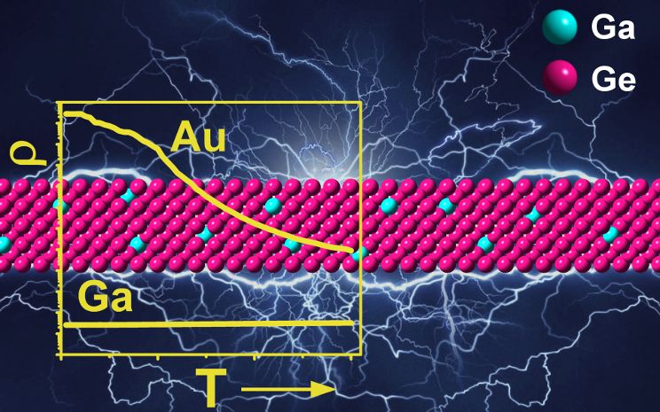
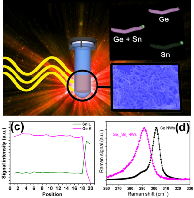
| Metastable materials, such as Ge/Sn or GaGe alloys, can also be prepared by our molecule-based approach combined with low temperature approaches including microwave and CVD techniques. For instance, our nanowires have been the first examples of bottom-up Ge1-xSnx nanowire growth with significant Sn incorporation. Controlling nucleation and metalorganic species are key for a successful and controllable synthesis. These Ge-based materials exhibit strongly altered physical properties. For instance, pure Ge is an indirect bandgap material but can be converted to a direct bandgap material by incorporation of high amounts of Sn (>~9 at%), which is well above the thermodynamic solubility limit of ~1 at%.
Selected papers: 7) “Epitaxial Ge0.81Sn0.19 Nanowires as Nanoscale Mid-Infrared Emitters” M.S. Seifner, A. Dijkstra, J. Bernardi. A. Steiger-Thirsfeld, M. Sistani, A. Lugstein, J. E. O. Haverkort, S. Barth* ACS Nano 2019, 13, 8047-8054 6) "Drastic Changes in Material Composition and Electrical Properties of Gallium-seeded Germanium Nanowires” M. S. Seifner, M. Sistani, I. Zivadinovic, M. G. Bartmann, A. Lugstein, S. Barth* Cryst. Growth Des.2019,19, 2531–2536. 5) "Direct Synthesis of Hyperdoped Germanium Nanowires" M. S. Seifner, M. Sistani, F. Porrati, G. DiPrima, P. Pertl, M. Huth, A. Lugstein, S. Barth* ACS Nano 2018, 12, 1236-1241. 4)"Pushing the composition limit of anisotropic Ge1−xSnx nanostructures and determination of their thermal stability" M. S. Seifner, S. Hernandez, J. Bernardi, A. Romano-Rodriguez, S. Barth* Chem. Mater. 2017, 29, 9802-9813. 3) “Microwave-assisted Ge1-xSnx nanowire synthesis: precursor species and growth regimes” M. S. Seifner, F. Biegger, A. Lugstein, J. Bernardi, S. Barth* Chem. Mater.2015, 27, 6125-6130. 2) “Microwave-assisted solution–liquid–solid growth of Ge1−xSnx nanowires with high tin content” S. Barth*, M. S. Seifner, J. Bernardi Chem. Commun. 2015, 51, 12282-12285. 1) “Neu zusammengesetzt: Gruppe-14-Elemente als Halbleiter“ S. Barth*, M. S. Seifner Nachrichten aus der Chemie2015, 1172-1175. |
|
Site-selective Growth / Nanowire Sensors
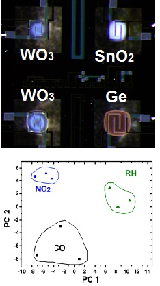
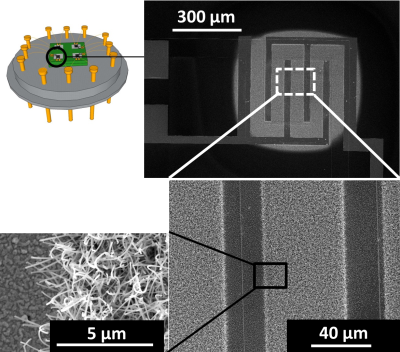
| Nanowire networks can be grown on micromembranes for sensor applications. The metal oxide nanowires grow exclusively on the heated area of a micro-machined chip. The same heater is essential for the post-growth sensor operation. A secondary circuit is located on top of the membrane heater and the interdigitates are bridged by the grown nanowires. This configuration allows a direct integration of nanowires in a functional device. The sensors are tested up to 1 month of continuous operation and show long term stability. The gases investigated with this configuration include carbon monoxide and ammonia in different humidity levels.
Selected papers: 1) "Site-specific growth and in situ integration of different nanowire material networks on a single chip: towards a nanowire-based electronic nose for gas detection" L. Hrachowina, G. Domenech-Gil, A. Pardo, M. S. Seifner, I. Gracia, C. Cane, A. Romano-Rodriguez,* S. Barth* ACS Sensors 2018, 3, 727-734. 2) "Humidity sensor based on Ge NWs selectively grown on suspended microhotplates" J. Sama*, M. S. Seifner, G. Domenech-Gil, J. Santander, C. Calaza, I. Gracia, S. Barth*, A. Romano-Rodriguez* Sens. Actuators B 2017, 243, 669-677. 3) "Gas sensors based on individual indium oxide nanowire" G. Domenech-Gil*, S. Barth, J. Sama, P. Pellegrino, I. Gracia, C. Cane, A. Romano-Rodriguez, Sens. Actuators B2017,238, 447-454. 4) "Site-selectively grown SnO2 NW networks on micromembranes for efficient ammonia sensing in humid conditions" J. Sama*, S. Barth, G. Domenech-Gil, J. D. Prades, N. Lopez, O. Casals, I. Gracia, C. Cane, A. Romano-Rodriguez* Sens. Actuators B, 2016, 232, 402-409. 5) “Localized growth and in situ integration of nanowires for device applications” S. Barth*, R. Jimenez-Diaz, J. Sama, J. D. Prades, I. Gracia, J. Santander, C. Cane, A. Romano-Rodriguez Chem. Commun. 2012, 48, 4734-4736. |
|
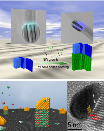
Growth studies
| We could recently show that defects from a metal can be transferred to a growing nanowire, which is the first example of an information transfer from a metal particle to a nanowire. A solid seed is important for this strategy to be effective. In addition, we could demonstrate that the pre-orientation of a seed material, which is not mixing with the growing nanowire material, can also promote the nanowire growth due to lattice matching of the growth seed and the forming nanowire.
Selected papers: 1) “Growth of monocrystalline In2O3 nanowires by seed orientation dependent vapour-solid-solid mechanism” S. Barth*, M. S. Seifner, J. Bernardi J. Mater. Chem. C 2014, 2, 5747-5751. 2) “Defect transfer from nanoparticles to nanowires” S. Barth, J. J. Boland, J. D. Holmes* Nano Lett. 2011, 11, 1550-1555. |
|
Thin Film and Nanoparticle Growth
Thin films are grown by low pressure chemical vapour deposition (LPCVD) or aerosol-assisted chemical vapour deposition (AACVD) using molecular precursors.
A prime example for the impact of the precursor's constitution on the depoeosited nanomaterial's composition can be illustrated using thioether functionalised group 13 alkoxides. The thermal decomposition of metal alkoxides typically leads to oxides; however, the use of thioether-functionalised alkoxides triggers the partial formation of sulphides without the presence of sulphates during the material conversion. Hence, secondary reactin channels can be triggered in materials synthesis when precursors are tailored to the targed material composition and the appropriated synthesis procedure.
Similar studies can be performed in solution phase processing for the preparation of oxide and sulphide nanoparticles.
Selected papers:
1) "Aerosol-assisted CVD of thioether-functionalised indium aminoalkoxides"
F. Biegger, F. Jungwirth, M. S. Seifner, C. Rameshan, S. Barth* Monatsh. Chem. - Chemical Monthly 2017, 148, 1385-1392.
2) "Thioether-functionalised gallium and indium alkoxides in materials synthesis"
F. Biegger, C. Rameshan, A. K. Opitz, J. Noll, T. Haunold, H. Lang, S. Barth*, New. J. Chem. 2016, 40, 6962-6969.
3) “Influence of precursor chemistry on CVD grown TiO2 coatings: differential cell growth and biocompatibility“
J. Altmayer, S. Barth*, S. Mathur* RSC Advances 2013, 3, 11234-11239.